Solar panel technology has come a long way in recent decades. Homeowners and businesses need to know the latest developments in the differences between monocrystalline vs polycrystalline solar panels — if there really are any — before buying.
Monocrystalline vs Polycrystalline Solar Panel: What’s the Difference?
Are you looking to purchase solar panels for your home or business but feel overwhelmed by all the choices available today?
For instance, you’ve probably read about the differences between monocrystalline vs polycrystalline solar panels and wonder if these differences really matter anymore.
While there are apparent contrasts between mono and poly solar modules, polycrystalline panels have recently undergone significant advances. Could polys be worth a more serious look for residential or business solar?
In this article on the differences between monocrystalline vs polycrystalline solar panels, find out everything you need to know about the latest upgrades to these residential and business solar options. We cover three types of differences:
- Solar power output
- Price per watt
- Carbon footprint
Our easy-to-understand tables of information on the differences between monocrystalline vs polycrystalline solar modules will help guide your purchasing decision
What are Solar Panels?
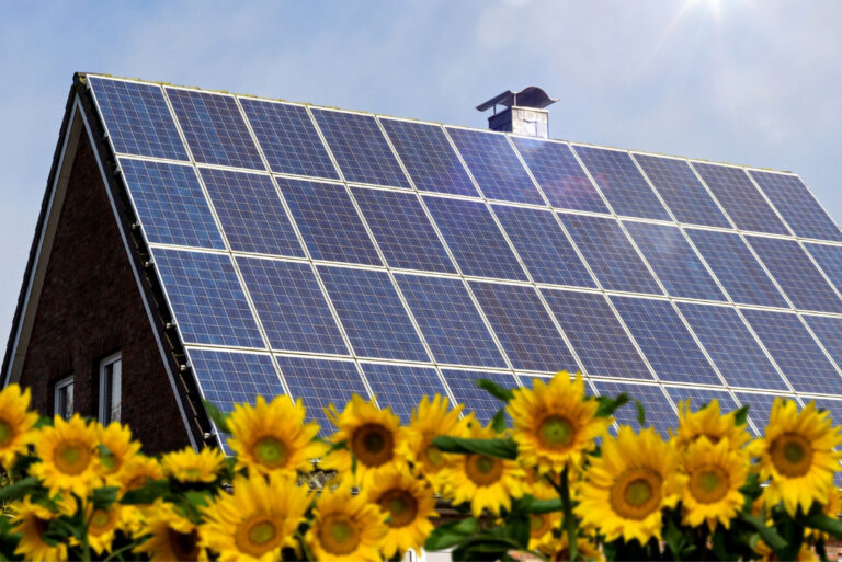
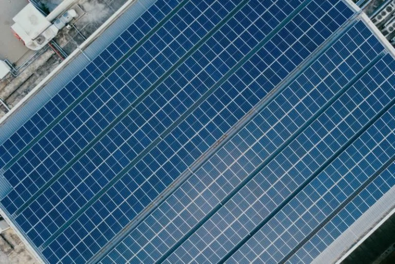
Have you seen sleek black or shiny blue glass-covered rectangular frames on roofs or on poles by highway construction sites?
Those devices are called solar panels. Other names for them are solar modules or photovoltaic (PV) panels.
Solar panels transform sunlight into direct current (DC) electrical energy that powers households, offices, or factories after inversion to alternating current (AC) electricity. Another type of panel may convert solar heat into thermal energy to warm water in pools or storage tanks.
In this article, we focus on solar panels that produce electricity.
What’s inside a solar panel?
Here’s a diagram showing the major layers inside a typical monocrystalline or polycrystalline PV module. Little has changed over time in the basic architecture of a solar panel.

What is a solar cell?
The workhorses of a solar panel are the multiple solar cells making up the central layer of a PV module as diagrammed above.
In the illustration, solar cells appear as blue rectangles separated by silver metal lines called ribbons, busbars, or fingers. The rows of silver diamonds indicate the absence of photovoltaic material on the corners of every solar cell. The diamonds are the hallmarks of monocrystalline solar panels manufactured in cylindrical containers (see below).
Inside the solar cells is where the solar-to-electrical energy transformation occurs.
The material responsible for the energy conversion in almost every solar cell on the market today is an ultra-thin silicon wafer composed of either:
- A single silicon crystal (mono) of high purity and flawless structure; or
- An irregular arrangement of multiple, imperfect and less pure silicon crystals (poly).
In the case of poly panels, some of the impurities are various silicon-containing compounds that did not undergo chemical conversion to unadulterated, free silicon.
Added to the silicon in both mono and poly modules are tiny amounts — at a parts per million (ppm) level — of other chemical elements, especially boron and phosphorus. This process is called doping. (Note: Parts per million means out of a million silicon atoms, only a handful are atoms of other elements.)
It’s the presence of these boron and phosphorus “impurities” in silicon that makes it chemically unstable. This means some outer electrons can easily move to other atoms under certain conditions. Specifically, the boron has too few electrons to stabilize it in the crystalline structure. Silicon doped with boron is called p-type.
On the other hand, phosphorus has too many electrons and isn’t stable in the crystalline lattice either. Silicon doped with phosphorus is called n-type.
As a result of the unstable electronic configurations of doped silicon, certain electrons circulate freely throughout the silicon crystal lattice when solar rays (photons) possessing high enough energy levels hit them.
In a properly doped solar cell, there is one side possessing an abundance of electrons and the other, a deficit of electrons (holes). The sun-excited electrons move in an organized way between these two ends at the p-n junction, forming an electrical circuit.
In other words, the solar cell generates electricity in the presence of sunlight. This process is known as the photovoltaic effect.
Here is a diagram illustrating the inner workings of a solar cell:

What is a silicon wafer?
The silicon wafers (slices) in solar cells are like the microchips or integrated circuits used in all electronic devices including your smartphone or laptop. They serve as the substrate (base) for various materials and operations. Electrochemical reactions occur on the wafer in solar cells. Alternatively, electronic systems function on them.
All silicon wafers are examples of semiconductors made of extremely thin slices of silicon.
The thickness of a typical silicon wafer for a solar cell is between 100-500 micrometers (microns). For comparison, one human hair is approximately 180 microns wide. (1 micron = 0.00004 in.)
In the case of a silicon wafer used as the substrate for a solar cell, the entire surface of the wafer is functional in capturing sunlight and converting it to electrical energy. However, in monocrystalline modules, the diamond-shaped corners are excluded from energy production.
Here is a diagram of a typical solar cell:

Why is silicon used in solar cells?
Silicon is used in solar cells because it’s an excellent semiconductor. This means it doesn’t conduct electricity as well as metals like copper (thus the prefix semi, meaning half or partly). Nor does it insulate against (stop) electrical transmission like some other materials such as glass or wood.
However, when certain substances are added (doped) to silicon, it becomes more electrically conductive. And it becomes able to convert one energy input (solar) into another (electricity). So it’s not an understatement to say that doped silicon serves as the cornerstone of the solar industry today.
Furthermore, in solar technology, one of the biggest advantages silicon has over other materials, especially metals, is that its resistance to electron flow decreases with increasing temperature. With the sun beating on solar panels thereby raising their temperature, you can understand why silicon is the preferred material in solar cells to generate and transmit electric current.
The current just moves with less restriction in doped silicon inside sun-baked solar cells. Differences in the temperature coefficients of PV panels mean some are better than others at doing this.
How is silicon purified?
Silicon must be purified before it can be used as a semiconductor. Furthermore, since most silicon in nature is bonded with other elements, it must also be extracted from these chemical compounds. Elemental (free) silicon is mostly bound up in substances called silicates or as silicon dioxide (silica) in sand or atmospheric dust.
Silicon purification: Molten salt electrolysis
So, to get solar-grade silicon from these compounds, molten salt electrolysis is a common, time-tested method to accomplish this. In this process, the silicon-containing substance in a molten state is literally split apart by an electric current, liberating silicon from its bonds with other atoms.
Silicon of 99.9% purity results from this technique which uses little energy, unlike other steps in making silicon wafers for solar cells.
Silicon purification: Trichlorosilane intermediate
Today, another method is commonly used to purify silicon, though in a roundabout way. Initially, impure silicon is chemically transformed into a specific silicon-containing compound that can be more easily purified later by distillation because it is a liquid (unlike solid silicon in sand). That compound, trichlorosilane, acts as the chemical intermediate in this step. Then, further chemical reactions convert trichlorosilane back to silicon in a much purer state.
The final product, pure silicon, is almost ready to be made into wafers for solar applications.
What are the types of silicon crystals used in solar cells?
Solar grade silicon is crystalline. It is a solid at room temperature. The chemical symbol Si stands for the element, silicon.
There are four categories of bulk silicon that can be used in PV panels. During manufacture, they are formed into ingots, ribbons, or wafers. (Note: Ingots are oblong blocks of metal cast from a molten state.)
- Monocrystalline silicon (c-Si)
The purest type of silicon, monocrystalline silicon is a single crystal cut from a cylindrical ingot in an energy-intensive process known as the Czochralski process. (The prefix mono means one.) When sliced thin, the wafer doesn’t fill an entire square of a solar cell, leaving gaps in all four corners.
- Polycrystalline (multi-crystalline) silicon (poly-Si, mc-Si)
Today, approximately 75% of poly-Si is commercially made by a modified Siemens process (see below). Or, leftover crystal fragments from c-Si manufacture can be melted together, forming poly-Si in a cube-shaped mold. (The prefix poly means many.)
- Ribbon silicon
A type of poly-Si, ribbon silicon is formed when molten poly-Si is physically stretched out to form flat, thin ribbons (films). This material is the basis of thin film solar panels.
- Mono-like-multi silicon (cast-mono)
Taking the best of both worlds, small seed crystals of silicon are grown in the cube-like casting chamber used to manufacture poly-Si. Once grown, the interior of the resulting crystal is pure cubed c-Si but the exterior is of poly-Si quality with a greater number of impurities. Cast-mono panels do not have non-photovoltaic diamond corners.
How are silicon wafers for solar cells made?
Today, the solar industry uses different techniques to manufacture monocrystalline vs. polycrystalline silicon wafers used in solar cells.
Both begin with impure, molten polysilicon feedstock made by the Siemens process or by a fluidized bed (FB) method. In these techniques, a chemical such as trichlorosilane in gaseous form is placed around a silicon rod acting as a seed crystal. In FB, at the “moderate” temperature of approximately 1,382°F, trichlorosilane breaks down, freeing silicon atoms. Pure silicon lands on the rod, enlarging it.
Chunks of polysilicon result from the Siemens process. Polysilicon granules are produced through the FB technique.
From molten polysilicon feedstock, monocrystalline silicon wafers are made through the Czochralski process (CZ-Si). Polycrystalline silicon wafers are produced via directional solidification (DS-Si) of polysilicon feedstock. Both of these methods are described below.
The major differences between CZ-Si and DS-Si involve:
- The way that polysilicon is melted
- How the polysilicon is shaped into an ingot
- The size of the final ingot
- How the ingots are shaped into bricks for slicing into silicon wafers.
How are monocrystalline silicon wafers made?
Monocrystalline solar panels contain solar cells made from a single crystal — referred to as a monocrystal — of pure silicon (c-Si). This means the entire crystal lattice is continuous (unbroken) even up to the edges.
The Czochralski process (CZ-Si), also called crystal pulling, is the most common method used today in the solar industry to make monocrystalline silicon wafers used in solar cells. It is the least expensive way to grow large silicon crystals.
Invented by chemist Jan Czochralski, this technique begins with a sample of molten polysilicon. Doping (usually with boron) occurs in this early stage.
A silicon monocrystal is pulled out of the polysilicon material (called the “melt” once heated) by dipping a rod of a pure silicon crystal in the cylindrical container of the molten poly-Si. Slowly, it grows into a single, large, and highly purified silicon crystal that is pulled out of the melt by raising and rotating the rod.
This process may take several days to complete.
Finally, a wire saw cuts the resulting mono ingot into super-thin silicon wafers which are then polished and cleaned. During the cutting process, 40-50% of the silicon is wasted. It may be used to manufacture polycrystalline solar cells (see below).
Here is a diagram of the Czochralski puller apparatus:

The Czochralski process is energy intensive, requiring high heat (2,574°F). Ingots up to 6 ft. long and 18 in. wide result.
Prior to 2005, circular solar wafers cut directly from the cylindrical ingots were formed. Now, most ingots undergo trimming into “pseudo-square” bricks to reduce waste and costs (see schematic below). Nevertheless, the completed monocrystalline silicon wafers still have rounded corners devoid of PV material.
Approximately 5,000-6,000 monocrystalline silicon wafers are sliced from one ingot.
Here’s a schematic of the entire process of making a monocrystalline solar wafer:

Monocrystalline solar grade silicon (Sog-Si) is not as pure as true c-Si needed to build electronics. Minor imperfections in the crystal lattice won’t affect solar performance like they would negatively impact the operation of sensitive electronic devices.
To achieve even higher purity than CZ-Si affords, the float zone (FZ) process is used. Silicon wafers made from FZ are used in electronics.
How are polycrystalline silicon wafers made?
Polycrystalline silicon (poly-Si) is made up of numerous small silicon crystals known as crystallites. They may be the leftover crystal bits and pieces from c-Si manufacture melted down together. Usually at this stage of production, a tiny amount of boron is added forming p-type silicon.
In the directional solidification (DS) process, polysilicon feedstock is melted down in a short and wide, cube-shaped crucible. Through a temperature gradient, the bottom of the crucible cools before the rest. Gradually, purer silicon solidifies from the bottom up along with the temperature gradient.
In the topmost molten part, most of the impurities reside. This part is not recycled back into feedstock, just like the bottom molten feedstock of the Czochralski cylinder is not.
From one DS ingot, 35,000-40,000 polycrystalline silicon wafers are cut.
Here’s a schematic of the DS polycrystalline silicon wafer manufacturing process:

In terms of crystal structure, polycrystalline silicon (poly-Si) is not as perfect as single-crystal monocrystalline silicon (c-Si). Nor is it like amorphous silicon (a-Si) that lacks a crystalline lattice of any significant size.
How is a monocrystalline solar cell made?
The manufacture of a monocrystalline solar cell begins with producing a single crystal of highly purified silicon through the Czochralski process (see above).
The cylindrical silicon ingot that results from that process is sliced ultra-thinly, washed, and polished into wafers.
Phosphorus is diffused across the surface of the wafers creating the p-n junction needed for the operation of an electric circuit in a photovoltaic system.
To reduce the over 30% of light reflected off their flat surface, solar wafers are texturized through etching. This process allows light rays to refract off (bounce around) many surfaces, thereby increasing the chance for absorption and boosting PV efficiency.
Furthermore, the solar wafers receive an anti-reflective coating (ARC) such as silicon nitride. This layer reduces the reflection of sunlight off the PV modules back to space so more can be absorbed by the solar cells, enhancing panel efficiency. Incidentally, ARCs are often applied on eyeglasses, sunglasses, or camera lenses.
This graph shows how effective ARCs are in reducing reflection off of solar cells:

To boost electrical conductivity, silver alloy ribbons and backing are applied to the wafers. They are now finished solar cells able to convert solar energy to electrical energy.
Metal also connects solar cells in rows and columns, forming the sheet of solar cells (usually 60+) encased in the middle layer of a solar panel (diagram above).
How is a polycrystalline solar cell made?
Polycrystalline solar cells could be made in one of two ways.
First, the Siemens or FB process (described above) produces relatively pure molten polycrystalline silicon. Instead of inserting a silicon rod as a seed crystal on which a single large silicon crystal forms (as in the Czochralski process), the melt is left to cool via a temperature gradient in a cube-like container. Once the melt hardens, leaving molten impurities on the top, a cube-shaped ingot of polycrystalline silicon remains, ready to be wire cut into wafers.
Alternatively, miscellaneous silicon crystal shards left over from the manufacture and cutting of monocrystalline silicon are melted together in a cube-like mold with a small quantity of boron, then resolidified. The resulting silicon block is cut into thin wafers (slices) of p-type silicon.
To form the critical p-n junction on a p-type silicon wafer, n-type dopant (like phosphorus) is diffused across the front surface.
Next comes the anti-reflective coating (ARC). As its name implies, this layer reduces the reflection of sunlight off the PV modules back to space.
In other words, the coating increases the absorption of radiant energy which leads to greater solar panel efficiency.
Today, ARC is often the chemical silicon nitride or boron nitride. Silicon or titanium dioxide are alternatives. It is applied to the module through a process called plasma-enhanced chemical vapor deposition.
To increase solar absorption further and boost solar panel efficiency, the silicon wafer may be texturized. This means its surface has been “roughened up” a bit to increase surface area on which solar rays can hit and to allow them to refract back on adjacent PV material.
Previously, only c-Si could be textured. But due to technological improvements, poly-Si can be textured today. This is another way differences between monocrystalline vs polycrystalline panels are becoming less important.
Finally, the silicon wafer is made into a solar cell by adding metal connections to the back and front. Using a silver paste, grid-like fingers and busbars are screen-printed on the surface. A full metal plate or grid is applied to the back.
To complete the metal connections and form electrodes in direct contact with the silicon wafer, the paste is heated at a very high temperature. In this manner, the passageway for electrical current is embedded in the silicon wafer.
A solar cell is born.
How are monocrystalline solar panels made?
After monocrystalline solar cells are prepared as described above, large numbers of them (typically 60 or more) are electrically connected together with wire or metal ribbons. Together, they make up the central layer of a solar panel.
The distinctive nature of a mono PV panel are the silver diamonds running along the columns of solar cells. Once a cylindrical (round) wafer from the ingot is placed on a square sheet, all four corners are devoid of photovoltaic material.
Encased in protective EVA plastic and placed under a glass cover with a backsheet all inside a metal frame, the PV module is complete.
Here is a schematic of the entire process:

How are polycrystalline solar panels made?
Square polycrystalline solar cells are prepared as described above. Large numbers of them (60+) are connected together with wire or metal ribbons forming an electrical circuit.
A sheet of solar cells is encased in protective EVA plastic and placed under a glass cover. Inside a metal frame and resting on a backsheet, the PV module is ready to generate electricity.
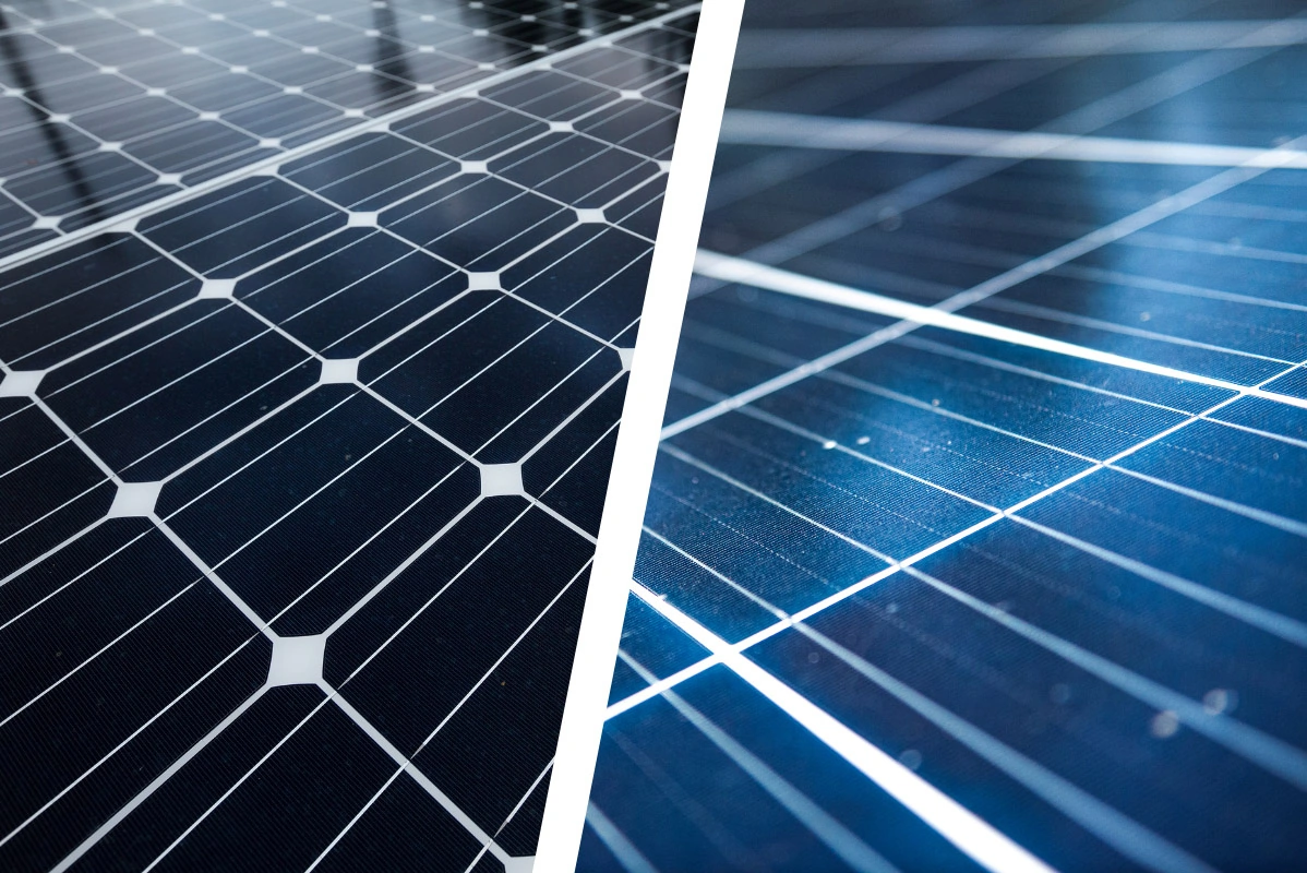
What are the superficial differences between monocrystalline vs polycrystalline solar panels?
Superficial differences between monocrystalline vs polycrystalline solar panels relate to the appearance of the PV modules.
Monos are black and characterized by solar cells with rounded edges. Polys have rectangular blue solar cells, giving them a bright, speckled look.
What are the solar power output performance differences between monocrystalline vs polycrystalline solar panels?
In terms of the characteristics that affect the solar power output performance of solar panels, differences between monocrystalline vs polycrystalline panels are not as pronounced as they once were.
Here is a summary table of monos vs polys graded on key performance metrics. These factors play significant roles in how well PV panels produce electricity.
Here’s a brief explanation on each of these parameters:
- Solar panel efficiency
In the simplest terms, efficiency is a measure of how well PV panels convert sunlight into electricity. The theoretical maximum efficiency of conventional monos and polys is approximately 33% (Shockley-Queisser Limit).
- Temperature coefficient of a solar panel
The temperature coefficient indicates how well a PV module withstands increases in temperature. The smaller the absolute (numerical) value (ignoring the negative sign which means reduction in efficiency), the better the panel.
- Degradation rate of a solar panel
Degradation rate shows how quickly PV panels will break down due to normal (mostly climatic) processes. A smaller rate is better.
Note: For more information on efficiency, temperature coefficient, and degradation rate, follow the hyperlinks given above.
| Performance Metric | Monocrystalline PV Panels | Polycrystalline PV Panels |
| Efficiency | Up to 22.8%; Average is 19-21% | Up to 19.5%; Average is 16-18% |
| Temperature Coefficient | As low as -0.29% | As low as -0.35% |
| Degradation Rate | As low as 0.2%/yr.; average 0.47%/yr. | In one study, systematically lower in poly-Si than c-Si; average is 0.61%/yr. |
Do the solar power output performance metric differences between monocrystalline vs polycrystalline solar panels really matter?
In 2022, the solar power output performance metric differences between monocrystalline and polycrystalline solar panels are so small compared to what they once were that these differences don’t really matter anymore.
As the table above suggests, it is possible today to buy a top-of-the-line poly that is performance competitive with a standard mono, especially in terms of efficiency.
Especially if you live in an area with moderate-to-cool temperatures (northern latitudes), the slightly higher temperature coefficient won’t have a huge effect on power output in a polycrystalline panel. Likewise, many types of heat-induced degradation will be minimized.
What is the price per watt difference between monocrystalline vs polycrystalline solar panels?
If you’re a home or business owner in the market for solar, you’ll be quoted price per watt by companies vying for your money. This difference between monos and polys has narrowed considerably over time. In fact, currently, there is significant overlap between them. It’s fair to say monocrystalline vs polycrystalline solar panels are price competitive in 2022 — and going forward!
For a year-by-year history of the differences in price per watt for monocrystalline vs polycrystalline solar panels, the International Energy Agency has an excellent interactive tool. The last four values shown in the table below are from this source.
| Metric | Monocrystalline PV Panels | Polycrystalline PV Panels |
| Price per Watt | $1.00-$1.501.30 (2011)0.90 (2014)0.60 (2017)0.30 (2019) | $0.90-$1.001.20 (2011)0.80 (2014)0.50 (2017)0.20 (2019) |
The shrinking gap in price between monos and ploys mirrors the overall drop in price of residential solar systems. Ten years ago, in 2012, it was $5.04/watt. In 2022, it’s $2.94/watt.
Does the price per watt difference between monocrystalline vs polycrystalline solar panels really matter?
The prices of both monocrystalline and polycrystalline solar panels have plummeted in recent years. Now, some monos are price competitive with the best polys.
If roof space is not a huge factor, polycrystalline panels may be your solution. However, by choosing high-efficiency polys, even the size of your roof won’t matter in many cases.
What is the carbon footprint difference between monocrystalline vs polycrystalline solar panels?
The amount of greenhouse gas emissions generated by the manufacturing of a solar panel is known as its carbon footprint.
The greater the quantity, the larger the contribution to our climate crisis from the panel’s production.
Note that for all PV panels on the market today, precious metals are needed. This requires fossil fuel-intensive mining and extraction. Environmental damage often results.
Does the carbon footprint difference between monocrystalline vs polycrystalline solar panels really matter?
The carbon footprint of monos is higher due to the intense heat required for several days during the making of each batch of silicon crystals. Fossil fuels are burned to produce this energy. The burning increases carbon emissions, fueling our climate crisis.
Additionally, the manufacturing process for monos is very wasteful of this energy. Approximately 40-50% of silicon manufactured in this way does not go into making c-Si modules. It is discarded. Some of it may go to produce polys.
Most PV panels are made in China where over 67% of all energy comes from fossil fuels, primarily coal (55% from coal in 2021). Plus, there are emissions from long-distance transport to other countries where the panels are installed.
Carbon-conscious home and business owners who wish to tread lightly on the Earth may opt for USA-made polycrystalline panels instead of Chinese-made monocrystalline PV modules.
Key takeaways on monocrystalline vs polycrystalline solar panels
Given all the choices today between monocrystalline vs polycrystalline solar panels, homeowners and businesses need to consider the latest technological developments before making their purchase.
Although monos have long been thought to be the best solar panels you could buy, this may not be the deal breaker for you especially if you’re budget-conscious and weighing prices per watt.
Or, if you’re a green consumer, carbon footprints of solar panels may really make a difference to you, in which case polys fit the bill.
Today, some polys power perform almost as well as monos — and for a lot less money and a lighter carbon footprint, too.
In 2022, homeowners and businesses alike have plenty of great solar options between monocrystalline vs polycrystalline solar panels. Begin your research with this article. Then, continue it with related resources and reviews on solar energy on this website.


![Eco-Worthy Solar Panel Review 2026 [Includes Buyer’s Guide]](https://greencoast.org/wp-content/uploads/2019/02/Eco-Worthy-Review-and-Buying-Guide-e1574180788859.jpg)